Last year, Altera provided a sneak preview of their forthcoming Stratix 10 devices (see Altera's Stratix 10 FPGAs & SoCs -- Breakthroughs in Performance, Integration, Density, and Security). Tempting and tantalizing as this sneak preview was, however, it was a little short on details.
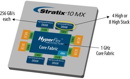
Well, Altera has now thrown the veils open a little wider, providing more concrete details regarding the Stratix 10 MX family of System-in-Package (SiP) devices. First of all we have the core monolithic FPGA fabric boasting up to 2,005,000 logic elements (LEs) and up to 679,680 adaptive logic modules (ALMs) that can run at up to 1 GHz. This core fabric also features a quad-core 64-bit ARM Cortex-A54 subsystem and peripherals running at up to 1.5 GHz.
 (Source: Altera)
In addition to hundreds of GPIOs, we also have up to 96 high-speed transceivers. But the real cream on the cake is the (up to) 16 GB of high-bandwidth DRAM memory (HBM). The four blocks of HBM -- along with the transceiver die -- are connected to the main FPGA die using Intel's embedded multi-die interconnect bridge (EMIB) technology, which provides ultra-high-density, ultra-high-speed interconnect between the HBMs and the FPGA fabric. In fact, the four HBM blocks provide an aggregate bandwidth of 1 TBps, which is 10X the bandwidth that can be achieved using discrete, off-package DRAM solutions while consuming much less power (see also this video).
Having up to 16 GB of in-package memory with a bandwidth of 1 TBps is going to be a game-changer for a wide range of applications, including 8K video, high performance computing (HPC), computer vision, big data, radar... the list goes on. This also dramatically reduces the footprint, routing, and power consumption at the board level. Quite apart from anything else, designers are now presented with a completely new memory hierarchy and architecture. Ridiculous as it sounds, we might actually find it difficult to come up with ways to take full advantage of the memory bandwidth that is available to us.
Sad to relate, these devices aren�t quite ready for purchase yet. When I asked the folks at Altera how this was different from last year's announcement, they pointed out that the nitty-gritty details of these devices are now fully documented to the extent that there are data sheets and whitepapers and part numbers against which one can place an order. These devices will be fully supported by the design software later this year, and sample devices will become available around the middle of 2017.
I must admit that I started to moan and groan a bit at this point, but the guys from Altera responded with a pertinent point that made me pause for thought. Even though the physical devices aren�t available just yet, the amount of information that is available means that designers can start planning future systems around these components. Strange as it seems, I really hadn't thought about things in quite this way before, but it does make sense now that I do think about it. What say you? Can you see one of these little scamps in your future (by which I mean a Stratix 10 MX SoC FPGA, not one of the folks from Altera)?
Related posts:
- Heterogeneous System Architecture: A New Computing Platform Infrastructure
- FPGA Debug in the Modern World
- MCU Guy, Meet FPGA; FPGA, Meet MCU Guy
- Madcap Ultrasound Engineers Send FPGA to 103,000 Feet
- Proceedings of the IEEE: Design Automation of Electronic Systems
- Programmable ASSP (pASSP) I/F Bridge for Mobile Image Sensors & Displays
- FPGA-Based Real-Time Spectrum Analyzer Sets New Record
— Max Maxfield, Editor of All Things Fun & Interesting 