Flex Logix' business model is that of licensing the technology to customers that want to include FPGA fabric in their SoCs and standard products.
Silicon for the EFLX family for 40ULP is in fabrication at TSMC and is expected to be validated during 4Q16. It is being aimed at providing reconfigurable RTL for microcontrollers and SoCs used in the Internet of Things. The inclusion of FPGA fabric can give a single die multiple functions and hardware accelerator functions and allows chips to be updated or changed at any time after fabrication, even in-system
Flex Logix, a startup founded in 2014, pitched its first FPGA fabric at system-on-chip (SoC) design on the 28nm HPM process launching in 2015 (see Put FPGAs in your SoCs). The latest family back fills the family and addresses a broader potential customer base.
Flex Logix� is offering both logic variant and DSP variant of its fabric on TSMC 40ULP and are specified for operation at both 1.1V and 0.9V with state retention down to 0.5V. The EFLX-100 IP cores/arrays in TSMC 40ULP require only 5 metal layers and support multiple clocks
EFLX-100 Logic IP core: 120 LUTs � each LUT is dual 4-input look-up-tables with dual flip flops � with reconfigurable interconnect, clocks, configuration logic/memory and 304 I/O in 0.13 square millimeters. Each is available in five different threshold voltage (VT) combinations to fit customers� designs and power/performance trade-offs. EFLX-100 DSP IP core: 88 LUTs and two MACs (22bit by 22bit multipler with pre-adder and 48-bit post-adder), with the same I/O and area as the EFLX-100 Logic IP core. This is also available in five different VT combinations.
The EFLX-100 IP cores can be arrayed to make larger arrays up to 5 by 5 with any combination of Logic and DSP IP cores inter-mixed. This means that there are 25 different possible array sizes/dimensions from 120 LUTs to 3000 LUTs; and hundreds of unique arrays possible considering combinations of Logic and DSP.
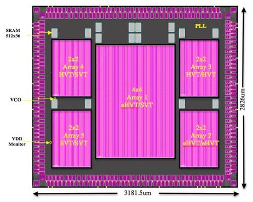
 GDS-II of TSMC 40ULP validation chip for EFLX-100. Source: Flex Logix.
Flex Logix uses an on-chip PLL, from True Circuits, to test at frequencies of 300MHz and above to confirm all functional and performance operation over the full temperature and voltage range. The validation chip is 9 square millimeters total.
Geoff Tate, CEO of Flex Logix, told EE Times Europe that the company has lead customer with silicon out of fab on the 28HPM process. But that the engagement with customers at 28nm had shown there was a market opportunity for a smaller anount of reconfigurable logic.
For this reason the base IP block on 40nm is about an order of magnitude smaller than the 2,500 LUT block offered at 28nm.
Tate said the company would not have considered it at launch but that 180-nanometer is also a possibility for Flex Logix with a smaller IP block. Meanwhile the company is already in development with a 100-LUT IP block for use on TSMC's 16FFC process node.
"We think embedded FPGA will be a pervasive market. It could be as big as embedded processors," said Tate.
One criticism of FPGA fabrics has been that while they help address the economics of low volume applications they are not power efficient compared with fully diffused circuitry.
Flex Logix has a couple of responses to that. One is that the Flex Logix fabric hierarchal architecture has been crafted to reduce the length of communications links and, thereby reduces the area required for interconnect and the number of metal layers required for implementation. This in turn reduces power consumption and allows improved performance compared to conventional FPGA architectures.
The second is to compare FPGA implementation with software on processor. "We are doing energy studies for MCU customers. These show we can beat [in terms of energy] software running on a processor core," said Tate.
Article originally posted on EE Times Europe.