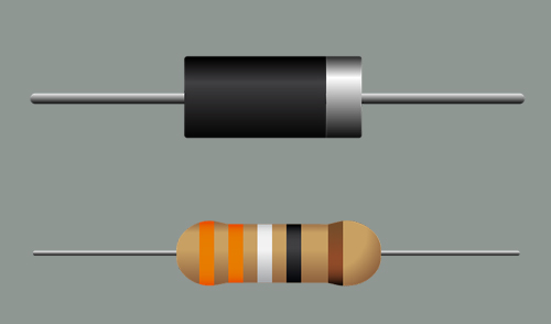
A crystal diode is a pn junction formed of a p-type semiconductor and an n-type semiconductor. For a p-type semiconductor, a trivalent element is doped in a semiconductor composed of a tetravalent element, such as boron is doped in silicon. The atom of the trivalent element can accept electrons to become negative ions. Correspondingly, a hole with a positive charge is generated in the covalent bond, and the movement of the hole can be exhibited outside due to the movement and transmission of electrons.
The n-type semiconductor is equivalent to doping a pentavalent elemental phosphorus in silicon. Due to the presence of a pentavalent element, electrons are increased, and the attraction of the atomic nucleus becomes a free electron.
Therefore, when a p-type semiconductor and an n-type semiconductor are combined, a diffusion phenomenon occurs due to the difference in concentration of electrons and holes between the two. When the diffusion phenomenon proceeds to a certain extent, the junction between the two will form a built-in electric field due to the neutralization of the charge, and the effect of the built-in electric field will cause the holes in the p-type semiconductor and the electrons in the n-type semiconductor to drift. That is, holes and electrons generate a flow in a direction opposite to the diffusion phenomenon due to the effect of the built-in electric field. This is the composition and working principle of the PN junction.

The diode has the characteristics of forward conduction and reverse cutoff. This characteristic is determined by the forward and reverse characteristics of the PN junction.
For the PN junction, the forward voltage is applied, which is equivalent to the diode plus forward voltage. P is connected to the positive terminal of the power supply. Obviously, the applied voltage is opposite to the field strength of the built-in electric field at this time.
This exacerbates the diffusion motion of holes and electrons and reduces drift motion. Since the amount of holes in the p region is much larger than the number of electrons, and the number of electrons in the n region is much larger than the amount of holes, the diffusion motion can become relatively strong, and the forward conduction characteristic is exhibited outside.
When the reverse voltage is applied to the PN junction, the built-in electric field is strengthened by the presence of the power supply. The strengthening of the built-in electric field hinders the diffusion, and also enhances the drift phenomenon. The enhancement of the drift phenomenon increases the width of the built-in electric field. Since the drift motion is caused by the mutual movement of the electrons in the p-region and the holes in the n-region, the remaining number is too small, and thus exhibits a small current conductivity.
In addition, the diode actually has a breakdown phenomenon. The breakdown of the diode within a certain range does not indicate the damage of the diode. When the diode plus reverse voltage reaches a certain value, the diode current will increase sharply, causing avalanche breakdown or Zener breakdown.
Both of these breakdowns have their own characteristics and have their own functions. There is not much to introduce here. The reason is necessarily the increase of movable free electrons and free holes in the PN junction. One is that high-energy carriers create new electron holes by collision of covalent bonds, and the other is that powerful electric fields directly destroy covalent bonds, producing electron and hole pairs.