TAIPEI — Chip scaling can double each year if the semiconductor industry pushes forward on a number of new technological fronts, according to TSMC Chairman Mark Liu, speaking at an industry event in Taiwan last week.
That expectation anticipates potentially faster growth for the semiconductor industry even as Moore’s Law is losing steam. Moore’s Law is the observation that transistor density in integrated circuits doubles every two years.
In the future, chipmakers will need to integrate memory and logic to create “true” 3D ICs that result in significant energy savings, said Liu at Semicon Taiwan last week. Moreover, domain-specific architectural innovations that allow software to configure hardware on the fly will also be key to achieving scaling advances.“The future of the semiconductor industry has never been so bright,” said Liu in a presentation at the Semicon event.
One of the megatrends for the electronics industry will be ubiquitous computing, allowing people to work anywhere, according to Liu. Autonomous vehicles will be another trend, requiring computing power to increase by 100 times from what is currently available today.
“Scaling will continue to 3 nm and 2 nm,” said Liu. “This will happen with EUV and new transistor structures like FinFET and new materials like high-k metal gate. EUV shows that lithography is no longer the limiting factor in scaling.”
New materials such as germanium graphene and molybdenum disulfide will also help boost transistor density in the future, he said.
Energy savings
In the past, die area, performance, and power were the key metrics for the semiconductor industry, according to Liu. Today, the new metric is energy efficiency.
“Density is already large enough for parallel computing,” he said. “What we need now is to reduce energy consumption.”
Liu noted that in data centers, nearly half of the cost of operation is consumption of electricity. That cost is exacerbated by AI, which requires intensive transfer of memory from storage.
The solution is to put memory and logic closer together with high-bandwidth interconnect, according to Liu.
TSMC’s advanced packaging technologies such as CoWoS have been a stopgap solution to this problem, but in the future, memory and logic will need to be stacked on top of each other to increase interconnect density by as much as 100 times, he said.
Hardware/software co-design
Another area awaiting advancement is software and hardware co-design, according to Liu.
While CPU architectures have been unchanged during the past 30 years, new special-purpose processors have become increasingly prominent. New cryptocurrency innovations have resulted in the creation of highly parallel processing devices.

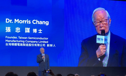
TSMC Founder and former Chairman and CEO Morris Chang speaks at the Semicon Taiwan event last week.
Source: SEMI
“Domain-specific architectures will come about to improve energy efficiency,” said Liu. “The problem is how to make them more flexible. How can we configure hardware on the fly?”
Rosy outlook
Liu’s comments were backed up by other speakers at Semicon Taiwan.
Morris Chang, the former chairman of TSMC, said that the world semiconductor industry will grow faster than global GDP in the foreseeable future. Chip industry sales will expand by about 5% to 6%, he said.
SEMI President and CEO Ajit Manocha, also speaking at the event, said that the chip industry is on track to reach sales of $500 billion in 2019 and $1 trillion by 2030.
“AI will be driving that,” he said.
— Alan Patterson covers the semiconductor industry for EE Times. He is based in Taiwan.

